Recent material technologies for GaN on GaN power devices
Yohei Otoki1), Hajime Fujikura1), Shinjiro Fujio1), Takehiro Yoshida1), Masatomo Shibata1), Yoshinobu Narita1), Takeshi Kimura1), Fumimasa Horikiri1), Hiroshi Ohta2), Tomoyoshi Mishima2)
SCIOCS1), Hosei University2)
https://www.sciocs.com/english/ otokiy@sc.sumitomo-chem.co.jp
GaN has been also used for AlGaN/GaN HEMT power devices on SiC substrates for amplifiers in wireless communication base stations. GaN-HEMTs on Si substrates have also been successful in high efficiency and cost competitive power supplies, with significant size reduction compared with Silicon.
A new generation of vertical GaN power devices is emerging, based on GaN epi grown on low dislocation density (low DD) GaN substrates. These vertical GaN devices promise significantly improved in performance compared with the initial HEMT devices [1], because of the improved junction quality which results from the lower DD in the GaN. This paper describes the impact of these defects on devices and recent material technologies for achieving vertical power devices at a reasonable cost.
The GaN substrates in this work were grown by the VAS method [2] which produces a low DD with a uniform distribution of dislocations. This DD uniformity is important, because clusters of dislocation significantly degrade the device performance through increased leakage current and reduced breakdown voltage VB. We characterized the electrical performance of both GaN Schottky diodes and GaN PN junction diodes on carefully prepared VAS GaN device samples [3][4].
(1) For the Schottky diodes, the extracted barrier heights, idealities, and reverse leakage currents on the VAS GaN samples were dramatically improved and almost ideal, compared with control samples fabricated on sapphire substrates with DD of over 1E8cm-2.[3]
(2) For the PN junction diodes, the extracted on-resistance Ron decreased with decreasing DD of the VAS GaN, and saturated at a DD value of about 1E5cm-2. The VB was independent of DD for DD less than 3E6cm-2 as shown in Fig.1 [4] . These results show that the DD of conventional VAS GaN substrate is good enough, but one order lower would be preferable.
A maskless three dimension growth (M-3D) method has been developed to produce even lower DD [5].
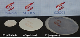
Increasing the diameter of the substrate and thickening the bulk crystal are effective in reducing manufacturing costs. Currently, 50 mm is still the most used size, but 100 mm diameter is also increasing. We have now demonstrated 150mm diameter VAS GaN substrates for the power device applications (Fig.2(a)) [6]. Furthermore, a bulk crystal with a thickness over 6 mm has been realized (Fig.2(b))[6].
The drift layer of a vertical power device needs to be thick (10um or more) and have high purity. By the MOCVD method, which is generally used for drift layer growth, increasing the purity reduces the growth rate, which increases costs proportionately. While the HVPE method has a growth rate of about two orders of magnitude higher than that of MOCVD, but excessive oxygen and silicon are incorporated into the crystal from the quartz reactor parts. Then, we have developed a quartz-free HVPE method (QF-HVPE) that dramatically suppresses the contamination from the quartz parts [7]. The purity of this crystal is so high that impurities cannot be detected by ordinary SIMS. As a result, a very high mobility over 1000 cm /Vs was successively obtained (Fig.3). By this method, a thick and high-purity drift layer can be produced at low cost.
Advances in GaN material quality and GaN growth technology, as well as innovations in GaN device design continue to drive remarkable performance improvements, and to uncover new GaN applications and markets and to reduce manufacturing costs. The VAS GaN method applied to GaN vertical power devices is an exciting recent example of this exciting industry trend.
ACCKOWLEDGEMENT
A part of this work has been supported by the Ministry of the Environment, Government of Japan.
REFERENCES
[1] https://www.eetimes.com/vertical-gan-devices-the-next-generation-of-power-electronics/#
[2]Y. Oshima, et al, phys. stat. sol. (a) 194, No. 2, 554 (2002)
[3]T. Hashizume, et al., Proc. of autumn meeting of Japanese Applied Physics 14p-a21-8 (2016).
[4]H. Ohta et. al., Jpn. J. Appl. Phys 60, SBBD09 (2021)
[5]T.Yoshida, et al, Jpn. J. Appl. Phys 59, 071007 (2020)
[6]H.Fujikura et. al., Jpn. J. Appl. Phys. 57, 065502(2018).
[7] H. Fujikura et al., Jpn. J. Appl. Phys 56, 085503 (2017)
Fig. 1. (Color online) Variations of (a) Ron and (b) VB with respect to the number of dislocations under the electrode. Copyright The Japan Society of Applied Physic (2020)[4]
(a) (b)
Fig.2 (a) Large size and (b) thick VAS-GaN substrates. Copyright The Japan Society of Applied Physic (2018)[6]
Fig.3 high purity GaN grown by QF-HVPE. Copyright The Japan Society of Applied Physic (2018)[7]